
Sustainability in the Semiconductor Industry: Key Takeaways
- Semiconductor fabs consume up to 15× more energy than traditional factories, making energy efficiency a top priority
- Leading manufacturers are investing in renewable-powered fabs, EUV lithography, and AI-driven process optimization to reduce emissions
- Each semiconductor wafer can require over 2,000 gallons of ultrapure water per day, highlighting the need for closed-loop water systems
- Scope 3 emissions, from suppliers and logistics, make up the majority of the industry’s carbon footprint
- Responsible sourcing of conflict minerals and improved traceability tools are essential for ESG compliance
- Companies can drive impact today through BOM optimization, excess inventory recovery, and sourcing from certified partners
The semiconductor industry consumes over 100 terawatt-hours of electricity each year, more than many entire countries.
As global demand for chips continues to surge across automotive, consumer, industrial, and medical sectors, so does the pressure to make semiconductor manufacturing cleaner, smarter, and more ethical.
In this guide, we will:
- Break down the key drivers behind the push for sustainability in the semiconductor industry
- Examine the environmental impact of chip manufacturing
- Highlight innovations in green semiconductor production
- Explore how recycling, circular supply chains, and material recovery are reshaping the industry
Why Sustainability Matters in the Semiconductor Industry
For many chipmakers, sustainability has shifted from a nice-to-have to a boardroom mandate.
Key reasons sustainability is critical in semiconductor manufacturing:
- Extreme resource intensity: Advanced fabs can consume up to 100 megawatt-hours per day and over 2,000 gallons of ultrapure water per wafer
- High emissions footprint: The industry emits potent greenhouse gases, including PFCs (perfluorocarbons) that have a global warming potential up to 12,000x greater than CO₂
- Global regulatory pressure: ESG reporting mandates (e.g., SEC climate disclosure rule, EU CSRD) require tracking Scope 1, 2, and 3 emissions
- End-customer expectations: Major OEMs demand greener chips to meet their own sustainability goals, especially in automotive and consumer electronics
- Supply chain risk: Water scarcity, energy constraints, and conflict minerals threaten continuity in production and sourcing
Why this matters now:
- Chip production is scaling fast: Global output is projected to double by 2030, meaning any inefficiency will be magnified without intervention
- Fabs are going green but unevenly: While some leaders like Intel and TSMC invest in renewables and circular waste systems, many suppliers lag behind
- Sustainability is linked to resilience: Cleaner, more efficient manufacturing processes reduce exposure to future regulations and resource shortages

Key Environmental Challenges in Chip Manufacturing
Modern chipmaking is a technological marvel, but it comes with a heavy environmental cost as each stage of semiconductor fabrication leaves a measurable footprint.
High Energy Consumption
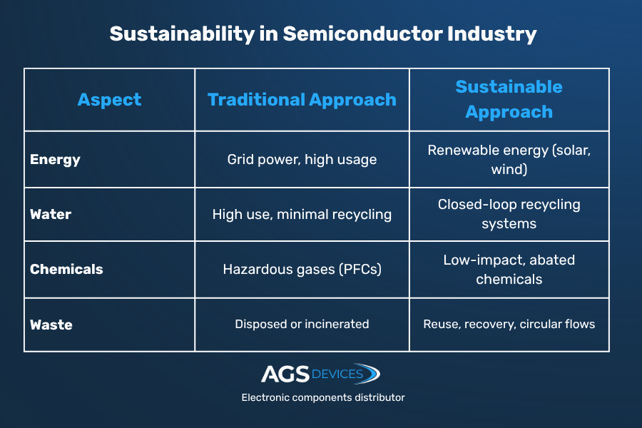
Fabrication plants (fabs) operate continuously, requiring enormous amounts of power to maintain cleanroom conditions and run precision equipment.
- When you compare a modern chip fab to a standard factory, the energy draw is startling, often ten to fifteen times higher, thanks to cleanrooms, precision tools, and non‑stop operation
- Key contributors: Photolithography, ion implantation, plasma etching, and wafer cleaning
- EUV isn’t just a technological leap; it’s changing the math on energy use per wafer, in some cases, slashing power needs by nearly half
Challenge: The transition to renewable-powered fabs is urgent but capital-intensive, especially for legacy fabs without energy-efficient infrastructure.
Water & Chemical Use
Water is essential for cleaning wafers, controlling humidity, and producing ultrapure inputs. But the volumes used are staggering.
- A single fab can use 2,000+ gallons of ultrapure water (UPW) per wafer per day.
- Chemicals like perfluorocarbons (PFCs), hydrofluoric acid, and photoresists are common and hazardous.
Did you know: Water-stressed regions (e.g., Taiwan, Arizona) are home to key fabs, making water use both an environmental and operational risk.
Waste & Emissions
Semiconductor production generates both direct and indirect emissions across the lifecycle.
- Direct emissions include greenhouse gases (like PFCs) and chemical runoff from etching and cleaning processes
- Indirect or Scope 3 emissions from raw material sourcing, supplier transport, and outsourced processes account for the majority of the carbon footprint
Difficulty: Most foundries lack full visibility into supplier-level emissions, complicating ESG reporting and risk management.
Innovations in Energy-Efficient Semiconductor Production
As fabrication becomes more complex, the industry is responding with smarter systems, renewable energy strategies, and breakthroughs that cut both emissions and operating costs.
Renewable-Powered Fabs
The future of semiconductors is solar, wind, and beyond.
- Major fabs are shifting toward 100% renewable energy to power 24/7 operations
- Intel, TSMC, Samsung, and others have committed to net-zero targets by sourcing electricity from solar, wind, and geothermal systems
- In 2022, Intel reported 93% renewable electricity use globally, with 100% in the U.S. and Europe
Consider this: A single fab can draw as much power as a small city. That kind of energy footprint isn’t just costly, it’s under growing regulatory scrutiny
Smart Manufacturing & AI Optimization
When AI steps onto the factory floor, efficiency levels up.
- Semiconductor leaders now deploy machine learning models to optimize etching, deposition, and lithography in real time
- By analyzing data at every wafer stage, fabs are actively slashing variation and cutting unnecessary power use, often before an engineer even spots an issue
- AI-driven maintenance has shown up to 20% reduction in tool-related energy losses
Why it matters: Smart automation doesn’t just make production faster; it makes it cleaner by minimizing rework, scrap, and overprocessing.
Low-Impact Lithography Techniques
Fewer steps, more efficiency, that’s the promise of next-gen lithography.
- EUV (Extreme Ultraviolet) lithography is replacing older multi-patterning methods, enabling denser chips with fewer processing steps
- Fewer steps = less energy per wafer, less chemical use, and higher yield
- ASML estimates that EUV reduces process complexity for nodes below 7nm, cutting both energy and material usage by 30–50%
Why it matters: In chipmaking, each process step isn’t just a technical hurdle; it’s another dent in your energy and emissions budget.
Sustainable Sourcing & Ethical Supply Chain Practices
Semiconductor sustainability doesn’t end at the fab; it extends across the global supply chain. From mining raw materials to component distribution, every step presents environmental and ethical risks.
Here’s how the industry is working to address them:
Why semiconductor sustainability can’t be ignored anymore:
- Scope 3 emissions accountability: Over 70% of a semiconductor company’s emissions typically come from upstream suppliers and logistics. Leading firms now require ESG reporting and carbon tracking from Tier 1 and Tier 2 suppliers
- Conflict-free minerals compliance: Tin, tantalum, tungsten, and cobalt are often sourced from high-risk regions. Responsible sourcing programs, like the Responsible Minerals Initiative (RMI), help verify ethical mining practices
- Traceability & material transparency: Companies are investing in blockchain tools and AI-driven supply chain platforms to track sourcing paths from mine to fab. This supports both regulatory compliance and brand trust, especially in automotive and defense markets
- Supplier ESG audits and ratings: OEMs and fabs now score suppliers on energy use, water efficiency, labor standards, and chemical handling. Failure to meet benchmarks can disqualify vendors from approved sourcing lists
- Sourcing resilience meets sustainability: Diversifying suppliers not only improves supply security, but it also reduces dependence on high-emission regions. Firms are reshoring key materials like silicon wafers to lower carbon and geopolitical risk
Why AGS Devices Is Your Partner in Sustainable Semiconductor Sourcing
Sustainability in the semiconductor industry isn’t a future initiative; it’s a present-day responsibility.
At AGS Devices, we help our customers balance innovation with sustainability by delivering components and sourcing strategies that reduce waste, improve visibility, and strengthen compliance.
Here’s how AGS Devices supports your sustainability goals:
- Certified, traceable sourcing: We partner with suppliers that meet RoHS, REACH, and conflict-free material standards
- Excess inventory & EOL solutions: Extend component lifecycles and reduce landfill waste through reverse logistics and last-time buys
- Optimized BOM support: Improve sourcing efficiency and material utilization with our expert BOM validation and part cross-referencing
- Transparent communications: Always know your lead times, alternative options, and sourcing risks, with full documentation
Besides semiconductors, we also provide electronic components such as:
Sustainability in the Semiconductor Industry: FAQs
What is the environmental impact of semiconductor manufacturing?
Semiconductor manufacturing is one of the most resource-intensive industrial processes. Fabs operate 24/7 and consume massive amounts of electricity, up to 15 times more than traditional factories. It’s easy to overlook, but each tiny wafer can demand thousands of gallons of ultrapure water, and that adds up fast, especially in drought-prone regions like Arizona.
How are chipmakers making semiconductor production more sustainable?
Leading chipmakers are adopting renewable energy, smart manufacturing technologies, and circular waste systems to reduce their environmental impact. Many fabs are transitioning to 100% clean electricity, while AI is being used to optimize processes and cut energy waste.
What does green semiconductor manufacturing involve?
Green semiconductor manufacturing focuses on reducing the environmental burden of chip production through energy efficiency, cleaner chemical usage, and closed-loop systems. It includes steps like powering fabs with renewables, using low-impact process chemicals, improving yield to reduce waste, and recycling materials like water and rare earths.
Why is sustainable sourcing important in the semiconductor industry?
Sustainable sourcing helps reduce Scope 3 emissions, the indirect emissions that occur across the supply chain, and minimizes the environmental and ethical risks tied to raw material extraction. Conflict minerals like tantalum and cobalt often come from high-risk areas, so traceability and responsible sourcing are essential.
Can smaller companies or OEMs improve sustainability without major infrastructure changes?
Absolutely. Not every sustainability improvement requires building a new fab. Companies can make meaningful progress by optimizing their bill of materials, selecting eco-certified components, and sourcing from vendors with transparent ESG policies.
What are Scope 1, 2, and 3 emissions in semiconductor manufacturing?
Scope 1 includes direct emissions from fab operations. Scope 2 covers indirect emissions from purchased energy. Scope 3 includes all other emissions, like raw material extraction, supplier processes, and logistics, which typically account for the largest share in semiconductor sustainability reporting.
Why is water use such a big issue in chip production?
Semiconductor fabs require ultrapure water to clean wafers at every stage. A single fab can use millions of gallons daily, often in water-stressed regions. Reducing and recycling water is critical to making chip production more sustainable.