Semiconductor Manufacturing: Key Points
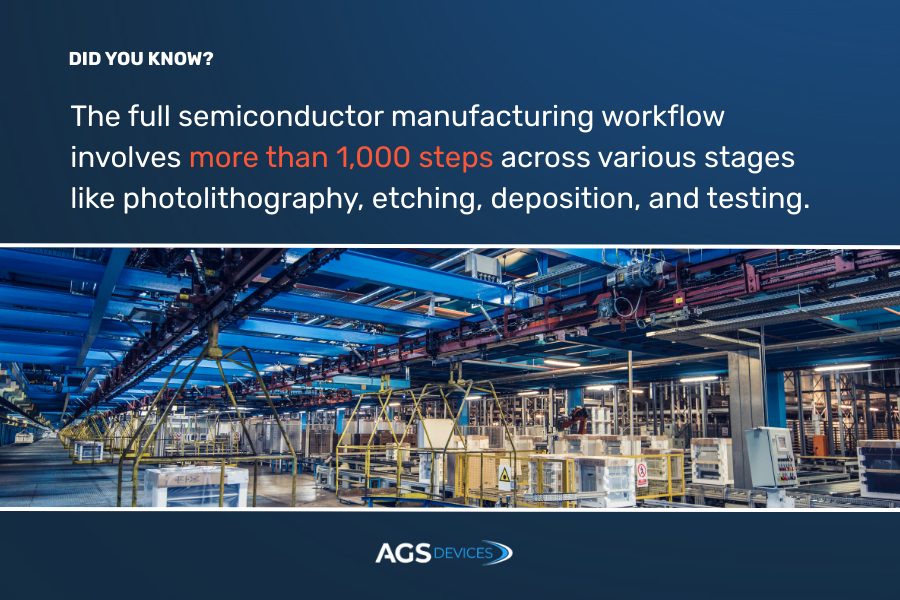
- Semiconductor fabrication is a highly precise, multi-step process involving deposition, patterning, doping, and packaging, all performed in controlled environments
- Silicon remains the base material for most chips, but alternatives like gallium nitride (GaN) are rising in high-efficiency and high-frequency applications
- Manufacturing hubs like Taiwan (TSMC), South Korea (Samsung), and the U.S. (Intel, GlobalFoundries) play critical roles in global supply
- Cleanroom conditions are critical, modern chip features are smaller than viruses, requiring extreme cleanliness and automation
- AGS Devices supports every stage of semiconductor sourcing, from finding hard-to-locate chips to planning around lead times and semiconductor shortages
The global semiconductor manufacturing market is expected to reach over $1191.1 billion by 2032, driven by demand for faster, more efficient chips in AI, automotive, and IoT applications.
But how exactly are semiconductors made, and what makes the process so complex?
This guide will break down:
- The full step-by-step semiconductor manufacturing process, from raw wafer to packaged chip
- The cleanroom standards and advanced technologies behind chip fabrication
- Where semiconductors are produced and why location matters in the supply chain
- The materials used, including silicon and compound semiconductors like GaN and GaAs
Step-by-Step Overview of the Semiconductor Manufacturing Process
Manufacturing a semiconductor chip is a multi-layered process that transforms raw silicon into intelligent, high-speed components.
Each step below plays a critical role in defining the chip’s performance, reliability, and end-use potential.
1. Wafer Fabrication and Doping
It all begins with transforming raw silicon into a blank canvas for microelectronic magic.
Here’s what happens in this foundational stage:
- Silicon is melted, purified, and formed into cylindrical ingots
- Ingots are sliced into thin wafers with ultra-smooth surfaces
- Wafers are doped with phosphorus or boron to modify conductivity
- Semiconductor doping defines N-type or P-type regions that enable transistor switching
- These doped regions allow chips to control electrical signals at high speeds
2. Photolithography and Etching
This is where the chip blueprint comes to life, with patterns smaller than a virus.
The steps include:
- UV light projects a circuit pattern onto the wafer’s photoresist coating
- Exposed areas are chemically developed to reveal design features
- Etching removes selected material to carve nanoscale structures
- These structures form electrical pathways between transistors
- Advanced photolithography enables billions of components on a single chip
3. Ion Implantation and Thin Film Deposition
Once the base pattern is set, it’s time to build up layers and fine-tune performance.
The process works as follows:
- Ion beams are fired into the wafer to fine-tune conductivity in key zones
- Conductive or insulating materials are deposited layer by layer
- Techniques include chemical vapor deposition (CVD) and atomic layer deposition (ALD)
- Layers are stacked with extreme precision to form transistors, gates, and interconnects
- This stage supports applications in high-performance CPUs, AI chips, and automotive ICs
4. Metallization and Interconnect Formation
Now it’s time to wire it all together.
These connections turn isolated components into a functioning system:
- Metal layers (usually copper or aluminum) are added to form interconnects
- Dielectric materials are layered between to prevent electrical shorts
- These interconnects act like the chip’s nervous system, carrying signals across billions of pathways
- Signal integrity is preserved through shielding and insulation
- In applications like data centers, strong interconnects reduce latency and power loss
5. Packaging and Final Testing
No semiconductor packaging is complete until it’s protected, tested, and ready to be integrated into a final product.
Here’s how the manufacturing is finalized:
- Wafers are cut (diced) into individual dies
- Each die is packaged with protective material and mounting pins or pads
- Thermal, electrical, and reliability tests screen for defects
- Only chips that pass stress and endurance tests are shipped
- Automotive-grade chips undergo rigorous qualification for heat, vibration, and signal accuracy
Where Are Semiconductors Made? A Look at Global Production Hubs
The semiconductor supply chain is global, but only a handful of countries dominate the most advanced stages of chip production.
The global hubs powering modern electronics include several countries.
1. Taiwan: The Leader in Advanced Chip Manufacturing
Taiwan is home to TSMC (Taiwan Semiconductor Manufacturing Company), the world’s largest and most advanced contract chipmaker. TSMC produces nearly 60% of the global foundry market and is the go-to source for cutting-edge nodes like 5 nm and 3 nm chips.
- TSMC manufactures chips for Apple, NVIDIA, Qualcomm, and other major tech companies.
- The country’s tight supply chain ecosystem supports fabless companies and rapid innovation.
Taiwan also faces geopolitical risks, making its central role in global electronics a topic of constant attention.
2. South Korea: High-Volume Memory and Logic Chips
South Korea is a powerhouse in DRAM and NAND flash memory, led by giants like Samsung Electronics and SK Hynix.
- Samsung is one of the few companies capable of manufacturing both advanced logic chips and memory at scale.
- The country invests heavily in R&D and is expanding its foundry capabilities to compete directly with TSMC.
3. United States: Design Leader and Growing Manufacturing Base
While the U.S. leads the world in semiconductor design (with companies like Intel, AMD, and Qualcomm), its manufacturing footprint has declined over the past few decades. However, the CHIPS and Science Act (2022) is reversing that trend.
- Intel is building advanced fabs in Arizona and Ohio to regain a competitive edge.
- The U.S. remains dominant in EDA software, chip architecture, and high-end design IP.
4. China: Scaling Up Domestic Production
China is investing billions to become self-reliant in semiconductors as part of its “Made in China 2025” initiative.
- Companies like SMIC (Semiconductor Manufacturing International Corporation) are increasing domestic production of 28 nm and 14 nm chips.
- U.S. export controls currently limit China’s access to extreme UV lithography, slowing progress at the most advanced nodes.
5. Europe and Japan: Specialized Manufacturing and Equipment
Beyond the U.S. and Asia, other global regions also play vital roles in the semiconductor ecosystem.
- Europe (led by STMicroelectronics and Infineon) focuses on automotive, industrial, and power semiconductors, with strong support from the EU’s “Chips Act.”
- Japan supplies essential semiconductor materials and manufacturing equipment and is home to legacy chipmakers like Renesas and Toshiba.
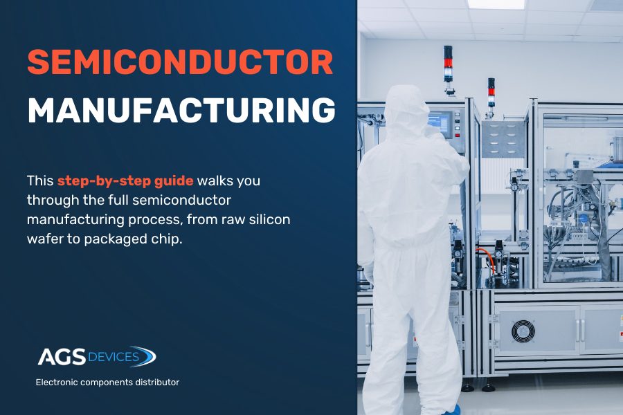
Semiconductor Manufacturing Technology and Cleanroom Standards
Building semiconductors isn’t just about precision, it’s about perfection. The scale of production operates at nanometer levels, meaning even the tiniest contaminant, vibration, or temperature shift can ruin an entire wafer.
Semiconductor Manufacturing Technology
The tools and equipment used in chip production are among the most advanced in the world. Some of the key technologies include:
- Photolithography machines: These systems use ultraviolet (UV) light to etch circuit patterns onto wafers. Extreme ultraviolet (EUV) lithography, used in the most advanced chips, prints features as small as 5 nanometers, smaller than a single virus particle.
- Ion implanters and etchers: These tools implant dopants into silicon and carve microscopic features with sub-nanometer accuracy, allowing manufacturers to tweak how current flows through individual transistors.
- Deposition and metrology systems: Chemical vapor deposition (CVD) and atomic layer deposition (ALD) build thin films layer by layer. Meanwhile, metrology tools like scanning electron microscopes inspect and measure features in real-time.
Fun fact: ASML’s EUV lithography machines cost over $200 million each and contain more than 100,000 components.
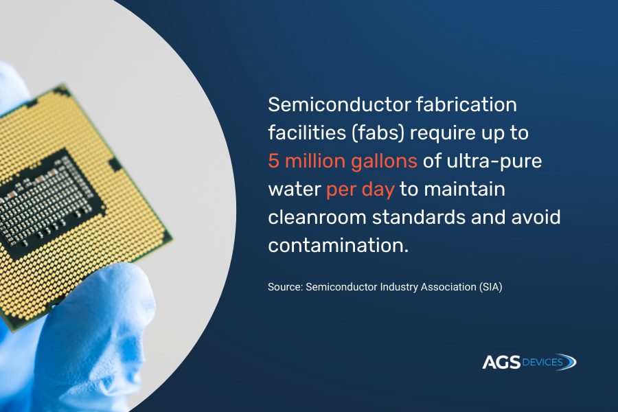
Cleanroom Standards in Semiconductor Facilities
Semiconductor fabs (fabrication plants) operate in ISO-certified cleanrooms, classified by how many particles of a certain size are allowed per cubic meter of air.
- Class 1 to Class 1000 cleanrooms are common in fabs. For comparison, a typical office has over 1 million particles per cubic meter, while cleanrooms aim for fewer than 10.
- Operators wear full-body suits (bunny suits) to reduce human contamination. Air inside the room is continuously filtered using HEPA or ULPA filters.
- Conditions such as temperature, humidity, and air pressure are rigorously controlled within narrow tolerances.
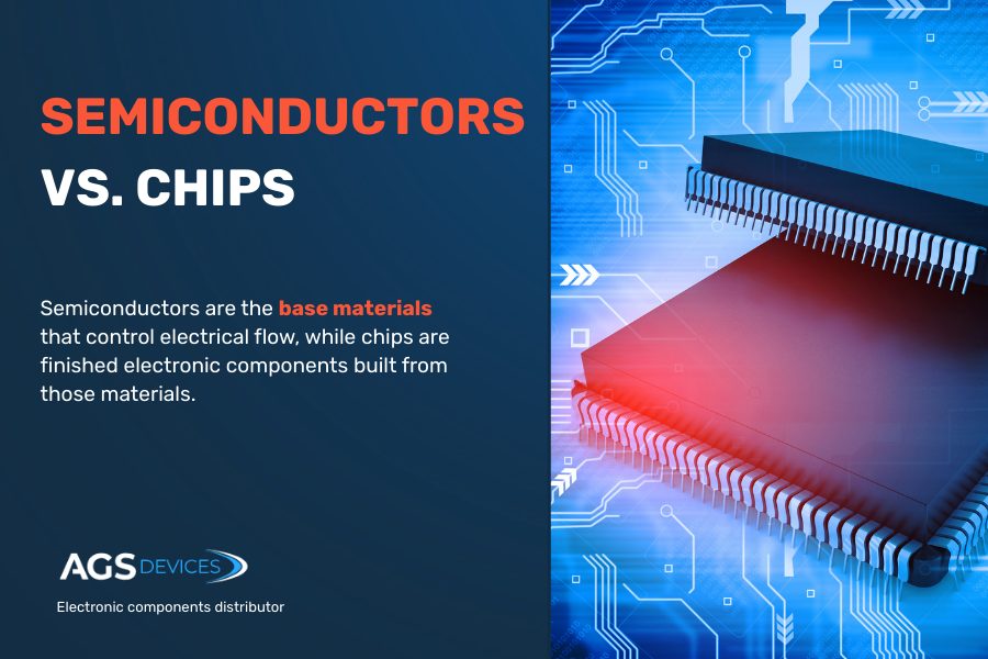
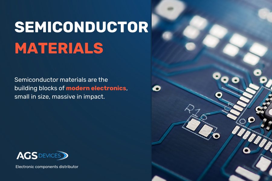
What Are Semiconductors Made Of?
Semiconductors are made from materials that can conduct electricity under some conditions but not others, making them perfect for controlling electrical signals in modern devices.
Silicon
Silicon (Si) is the most widely used semiconductor material in the world. The majority of semiconductor devices are built on silicon wafers due to its abundance, affordability, and excellent electrical properties.
- It’s a group IV element on the periodic table, with four valence electrons, ideal for forming the crystal lattice required for integrated circuits.
- Silicon’s stability and ability to be doped with precision make it ideal for high-volume, reliable production.
Other Semiconductor Materials
While silicon dominates, several other materials are used in specific applications where performance or efficiency must exceed what silicon can provide.
These other materials include:
Gallium arsenide (GaAs):
- Offers higher electron mobility than silicon, perfect for high-speed, high-frequency applications.
- Commonly used in RF chips for smartphones, radar systems, and satellite communications.
Silicon carbide (SiC):
- Known for its ability to withstand high voltages, high temperatures, and harsh environments.
- Used in power electronics for electric vehicles (EVs), industrial equipment, and renewable energy systems.
Gallium nitride (GaN):
- High efficiency and fast switching speeds make GaN a go-to for compact power supplies, fast chargers, and 5G infrastructure.
- GaN semiconductors are revolutionizing power conversion technology.
Germanium (Ge):
- Once widely used before silicon became dominant. Still relevant in some specialized applications due to high electron mobility.
- Occasionally used in photodetectors and solar cells.
Why AGS Devices Is a Trusted Partner for Semiconductor Sourcing
At AGS Devices, we understand that the quality and availability of semiconductors can make or break a project.
Whether you’re sourcing high-performance silicon wafers, GaN power components, or niche compound semiconductors, our global supplier network and robust quality assurance protocols ensure you’re getting the right part at the right time, every time.
We also support your full component sourcing needs, offering:
- BOM Management
- Shortage and Obsolescence Solutions
- Sourcing and Procurement
- Excess Material Acquisition
Our team is deeply familiar with the demands of industries like aerospace, medical technology, automotive, and industrial automation, and we tailor solutions to meet your exact needs.
Semiconductor Manufacturing: FAQs
Have questions about how semiconductors are made, where they’re produced, or what materials are used? Here are clear answers to the most common queries engineers and sourcing teams are asking.
What is semiconductor manufacturing?
It’s the process of creating integrated circuits (ICs) from raw materials like silicon. It includes multiple precise steps such as doping, etching, layering, and testing.
How are semiconductors made step by step?
The process includes wafer fabrication, photolithography, ion implantation, metallization, packaging, and testing. Each step builds the chip’s internal structures and ensures performance.
Why are cleanrooms important in chip manufacturing?
Because features are measured in nanometers, even a single particle of dust can destroy a chip. Cleanrooms filter air and regulate humidity, pressure, and temperature to prevent contamination.
What is the most used material in semiconductor manufacturing?
Silicon is the dominant material due to its abundance, stability, and excellent electrical characteristics. Other materials like GaN and SiC are used for specialized applications.
Which countries lead in semiconductor production?
Taiwan, South Korea, the U.S., and China are key hubs. Taiwan’s TSMC leads in advanced chips, while the U.S. focuses on design and is investing in new fab capacity.
Can AGS Devices help source semiconductor materials or chips?
Yes. AGS Devices provides global sourcing for silicon wafers, compound semiconductors, and hard-to-find components, with full support for BOM optimization and shortage management.