Semiconductor Packaging: Key Takeaways
- Up to 70% of performance issues in electronics can be traced back to thermal or signal failures, both directly influenced by packaging
- Advanced packaging types like BGA and CSP are essential for high-speed, compact designs, but require more precise sourcing and assembly
- Packaging affects availability as a single chip model may have 3+ package variations
- Engineers make critical packaging choices early, but procurement must validate them for cost, compatibility, and supply chain impact
- Packaging drives footprint, heat management, and manufacturability as choosing the wrong one can delay production or require board redesign
Over 50% of semiconductor failures are linked to packaging-related issues such as overheating, poor connectivity, or mechanical stress.
Whether you’re designing for speed, size, or thermal control, the packaging determines how well a chip performs and how easily it can be sourced and assembled.
In this guide, we’ll cover:
- What semiconductor packaging is and its role in chip protection
- How different packaging types impact design, thermal performance, and sourcing complexity
- The full packaging process, from wafer dicing to final inspection
- When to consider advanced packaging and how it supports high-speed, compact systems
- Why engineers and sourcing teams must align early to avoid costly redesigns and delay
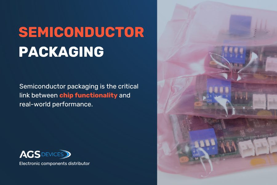
The Role of Packaging in Chip Protection
Semiconductor packaging is more than just a physical casing; it’s a critical component that protects the chip, enables connectivity, and maintains performance in real-world environments.
Once a silicon wafer is diced into individual chips (or “dies”), those bare chips are:
- Electrically inactive
- Mechanically fragile
- Highly sensitive to moisture, dust, and heat
What Does Semiconductor Packaging Actually Do?
The package provides a protective and functional interface between the silicon die and the rest of the system.
It serves several vital roles as it:
- Shields the chip from environmental stress, mechanical damage, and contamination
- Connects the chip to external circuits via pins, leads, or solder balls
- Helps dissipate heat to prevent performance issues and extend the chip’s lifespan
- Provides structural integrity and enables secure mounting to PCBs
The Semiconductor Packaging Process Step by Step
Transforming a silicon wafer into a reliable, functional chip ready for integration doesn’t happen overnight.
Here’s a step-by-step look at how chips are packaged and why each stage matters in sourcing and design.
Step 1: Wafer Dicing
The journey begins with a completed wafer containing hundreds (or thousands) of identical ICs.
In the first step, you should know that:
- Precision blades or lasers are used to cut the wafer into individual dies
- Each die is a tiny chip, just a few millimeters wide, and needs extreme care during handling to avoid breakage
Step 2: Die Attach
Once separated, the dies must be mounted securely onto a base.
At this stage, it’s important to understand how the foundation for future electrical and mechanical performance is set:
- Using a thermally conductive adhesive or solder, each die is placed onto a lead frame, substrate, or interposer
- This forms the foundation for both mechanical support and electrical connections
Step 3: Wire Bonding or Flip-Chip Interconnect
Now the die must be connected to the rest of the system.
Depending on performance needs, manufacturers use one of two main interconnection methods:
- For most traditional packages, ultra-thin wires (often gold or aluminum) are bonded from the die to the package leads
- For high-performance designs, flip-chip bonding is used, where the die is flipped and connected directly via solder bumps, reducing signal path length and improving thermal efficiency
Step 4: Encapsulation
Once connected, the entire assembly needs protection.
The die and wires are encapsulated in a mold compound (usually epoxy), shielding it from:
- Moisture
- Physical damage
- Contamination during assembly
- Encapsulation also helps improve the chip’s mechanical strength and handling safety.
Step 5: Testing & Inspection
Before shipping any chip, it must be verified for reliability and function.
This step includes:
- Electrical testing (to confirm performance and power characteristics)
- Visual and automated optical inspection (AOI) to detect physical or soldering defects
- Testing ensures only functional, spec-compliant chips move forward to inventory and distribution
Step 6: Marking, Trimming, and Final Packing
With testing complete, the chips are prepped for delivery and integration.
This final stage involves:
- Marking (model number, lot code, and traceability data)
- Lead trimming and forming, if needed, to match mounting requirements
Types of Semiconductor Packaging Explained
Semiconductor packages come in many shapes, sizes, and structures, each designed to meet specific performance, space, and assembly requirements.
Below are the most widely used semiconductor packaging types, along with where and why they’re typically used.
DIP (Dual Inline Package)
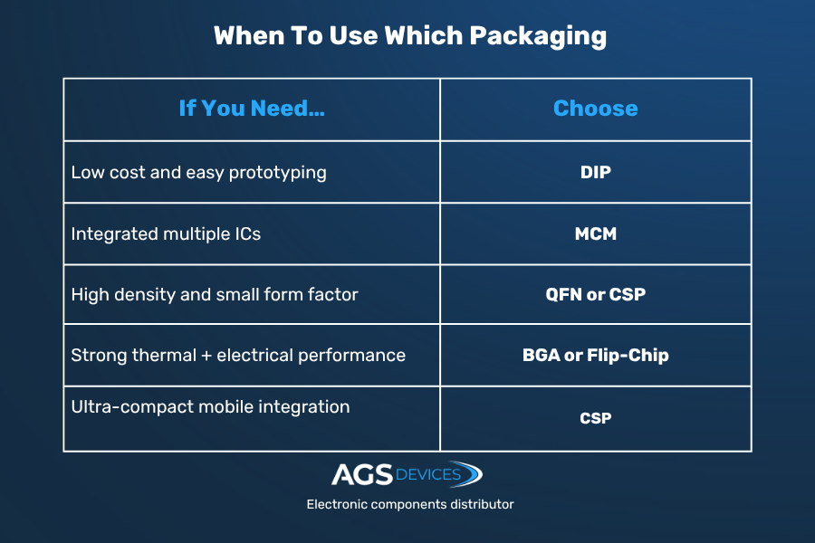
One of the oldest packaging types, DIP is still used in prototyping and legacy systems thanks to its simplicity and ease of handling.
- Through-hole package with two parallel rows of pins
- Common in legacy designs, prototyping, and education
- Large footprint but easy to handle and solder
- Often found in power supplies and early microcontrollers
QFN (Quad Flat No-Lead)
QFN packages are a go-to for modern compact devices that require efficient heat dissipation and minimal board space.
- Surface-mount package with no protruding leads
- Compact and thermally efficient
- Ideal for high-density PCB layouts
- Popular in consumer electronics and RF applications
BGA (Ball Grid Array)
Designed for high-performance chips, BGA packages provide excellent thermal and electrical characteristics in exchange for more complex assembly.
- Uses solder balls arranged in a grid under the chip
- Excellent for high-pin-count and high-speed applications
- Superior thermal and electrical performance
- Requires precise reflow and inspection equipment
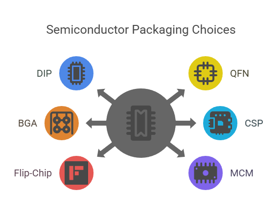
CSP (Chip Scale Package)
When space is at a premium, CSP allows the chip to take up almost no more space than the die itself—perfect for ultra-compact designs.
- Package size is nearly equal to the size of the die
- Minimizes board space and improves electrical performance
- Common in smartphones, IoT, and space-constrained devices
Flip-Chip
Flip-chip packaging flips the die upside down for a direct connection to the substrate, making it ideal for high-speed, high-power applications.
- Die is flipped and connected directly to the substrate via bumps
- Reduces parasitic inductance and improves heat dissipation
- Used in high-performance processors, GPUs, and ASICs
MCM (Multi-Chip Module)
MCMs combine multiple dies in one package, enabling more powerful and integrated solutions for advanced systems.
- Contains multiple ICs within a single package
- Enables complex functionality and compact integration
- Common in automotive, aerospace, and high-end computing
How Engineers Influence Chip Packaging Decisions
While procurement and sourcing teams handle availability and logistics, engineers play a central role in shaping packaging decisions, often as early as the concept and prototyping stages.
These decisions are driven by a set of engineering priorities, which include:
- Thermal behavior: Engineers model how the chip will dissipate heat under different workloads. High-power designs may require BGA, flip-chip, or even active cooling-compatible packages.
- Signal integrity: For high-speed applications, engineers evaluate packages that minimize parasitic inductance and interference (e.g., QFN or flip-chip over traditional wire-bond packages).
- Mechanical durability: In rugged or mobile environments, engineers may prioritize robust encapsulation or shock-resistant packages like molded lead-frame or CSP.
- Size & layout constraints: PCB real estate is limited, especially in consumer devices, IoT, and aerospace. Engineers must choose packages that fit the layout without compromising functionality.
- Manufacturing process compatibility: Engineers collaborate with assembly teams to ensure package types align with available pick-and-place, reflow, and inspection processes.
AGS Devices Is Your Strategic Partner From Packaging to Product Success
Semiconductor packaging isn’t just a design detail; it’s a key driver of product performance, manufacturability, and sourcing success.
The right package can reduce thermal risk, optimize layout, and streamline production. The wrong one can create delays, compatibility issues, or sourcing bottlenecks.
At AGS Devices, we go beyond just delivering components. We help you make informed packaging decisions that align with your electrical, mechanical, and supply chain requirements.
We support your entire procurement workflow with:
Whether you’re scaling production or troubleshooting a high-mix assembly, AGS Devices provide the precision, tools, and expertise to keep your builds on track.
Semiconductor Packaging FAQs
If you still have some additional questions about semiconductor packaging, these might answer some of your doubts.
What is semiconductor packaging and why is it important?
Semiconductor packaging protects the chip, enables electrical connections, and manages heat during operation.
What are the most common types of semiconductor packages?
Common types include DIP, QFN, BGA, CSP, flip-chip, and MCM, each suited to different performance and size needs.
How does the semiconductor packaging process work?
It includes wafer dicing, die attach, wire bonding or flip-chip, encapsulation, and final testing.
What is advanced packaging for semiconductors?
Advanced packaging includes 2.5D/3D ICs and fan-out methods, used in high-speed or space-limited applications.
What does a semiconductor packaging engineer do?
They design and select packaging to optimize chip performance, reliability, and manufacturability.
What factors affect packaging selection during sourcing?
Availability, cost, lead time, thermal needs, and assembly compatibility all influence package choice.