N-Type Semiconductors: Key Takeaways
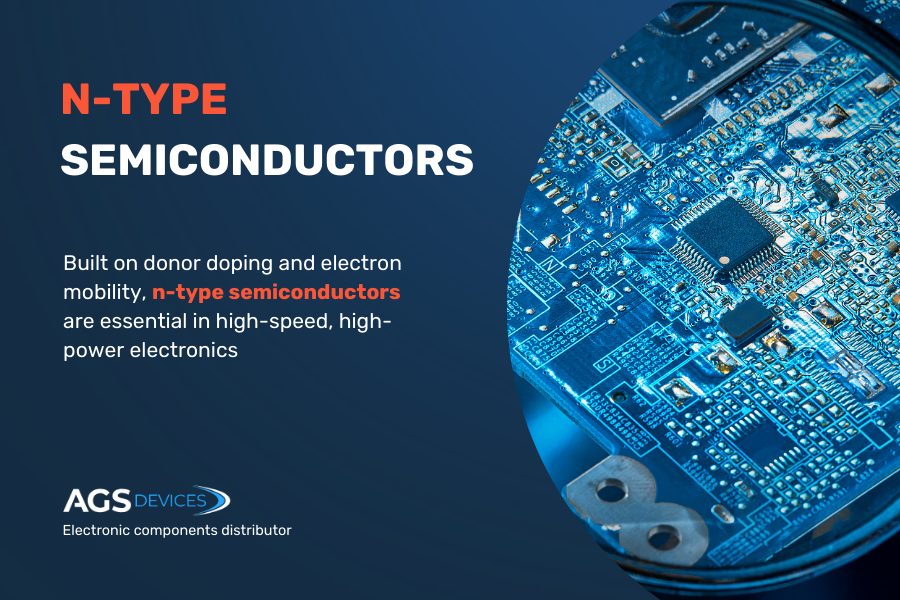
- N-type semiconductors conduct electricity using free electrons introduced via donor doping
- Electrons are the majority carriers, making n-type materials faster and more efficient than p-type in many applications
- Common examples include silicon doped with phosphorus, GaN for power electronics, and InP for high-frequency optical systems
- N-type semiconductors feature a shifted Fermi level, reduced energy gap, and high conductivity under applied voltage
The global wide bandgap semiconductor market (including N-type semiconductors) is projected to reach $5.5 billion by 2027, growing at 20% CAGR, driven largely by EVs and RF demand.
N-type semiconductors are at the heart of this shift. You’ll find them in everything from your laptop’s CPU to power inverters in EVs and satellites.
But what makes them so essential?
The answer lies in their structure: by doping pure semiconductors with donor atoms, N-type materials gain free electrons that allow for fast, low-resistance electrical conduction.
In this guide, we break down:
- How N-type semiconductors work at the atomic level
- Which materials and dopants matter most
- Real-world examples and applications
- Why sourcing the right components matters for performance and reliability
How N-Type Semiconductors Work
N-type semiconductors conduct electricity through free electrons, not holes.
In this section, we’re going to explain how they work in detail.
1. Doping Introduces Free Electrons
Pure semiconductors (like silicon) have limited conductivity at room temperature.
To boost performance, they’re “doped” with group V elements, such as phosphorus, arsenic, or antimony, which each have five valence electrons.
This is what happens at the atomic level:
- Four electrons bond with surrounding silicon atoms
- The fifth electron becomes a free carrier, easily moving under an electric field
- This creates a surplus of negatively charged electrons, hence the term “N-type” (for negative)
2. Electrons As Majority Carriers
Unlike p-type semiconductors (which rely on holes), N-type semiconductors use electrons as their main charge carriers.
Key characteristics include:
- Electrons as the majority carriers
- Holes (missing electrons) as minority carriers
Since electrons move more easily than holes, N-type materials have higher mobility, making them faster and more efficient for signal transmission and switching.
3. Energy Band Behavior
Doping shifts the material’s Fermi level (the probability threshold of electron occupancy) closer to the conduction band, reducing the energy needed for electrons to flow.
- Electrons from donor atoms occupy energy levels just below the conduction band
- A small thermal excitation is enough to push them into the conduction band, enabling current flow
This narrow energy gap enables low-resistance conduction under normal operating conditions.
4. Response to Electric Fields
When voltage is applied:
- Free electrons move from the negative terminal (cathode) toward the positive terminal (anode)
- This creates current flow through the semiconductor
This behavior forms the basis for how N-type materials operate inside:
- Diodes (forward bias enables electron flow)
- MOSFETs (n-channel types use electrons to form conduction paths)
- Photodetectors and amplifiers in sensitive electronics
N-Type Semiconductor Examples in the Real World
N-type semiconductors are the backbone of modern electronics, from the chips in your smartphone to mission-critical aerospace systems.
Here are the most common and impactful real-world examples.
1. Silicon Doped With Phosphorus (Si:P)
The industry standard for digital electronics, Si:P, is the foundational N-type semiconductor behind modern logic and memory devices.
- Use cases: Microprocessors, memory chips, power ICs
- Why this is important: Silicon doped with phosphorus is the most widely used N-type material in integrated circuits (ICs) and logic devices.
- Example: Every Intel or AMD processor contains billions of transistors made using N-type silicon
2. Gallium Nitride (GaN)
GaN’s wide bandgap and high-efficiency switching have made it the go-to N-type material for next-generation power and RF systems.
- Use cases: Power electronics, RF amplifiers, high-frequency converters
- Why this is important: GaN is a wide-bandgap N-type semiconductor known for high breakdown voltage and low on-resistance.
- Example: GaN is found in 5G base stations, fast chargers, and EV onboard chargers
3. Indium Phosphide (InP)
When speed, frequency, and precision matter most, InP delivers, especially in optical and aerospace-grade semiconductor designs.
- Use case: High-speed fiber optics, laser diodes, space-grade electronics
- Why this is important: InP supports extremely fast electron movement, making it the preferred N-type material for high-frequency and photonic devices
- Example: Used in data center optical transceivers, satellite communication systems, and quantum sensors
4. Zinc Oxide (ZnO)
ZnO combines semiconducting and optoelectronic properties, making it ideal for transparent and UV-sensitive applications.
- Use cases: Transparent electronics, UV sensors, piezoelectric devices
- Why this is important: ZnO is an N-type material that offers optical transparency and sensitivity to ultraviolet light
- Example: Found in transparent displays, solar cells, and smart windows
5. Tin Oxide (SnO₂)
Known for its transparency and sensitivity to environmental changes, SnO₂ is a reliable N-type material in sensor and interface technologies.
- Use cases: Gas sensors, touchscreens, transparent electrodes
- Why it matters: N-type behavior in SnO₂ allows it to detect environmental changes (like gas concentrations) by measuring shifts in conductivity
- Example: Used in indoor air quality monitors, touch-sensitive control panels, and transparent electrodes for smart glass systems
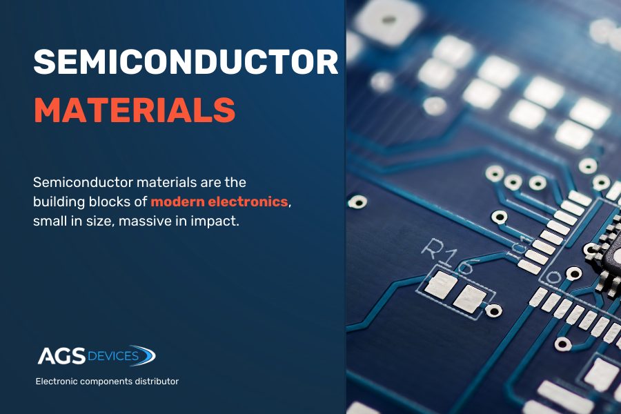
Materials and Structure of N-Type Semiconductors
The performance of any N-type semiconductor starts with its atomic structure and dopant materials.
Base Materials: The Semiconductor Host
Most n-type semiconductors begin with intrinsic (pure) semiconductor materials like:
- Silicon (Si): The most widely used; low cost, stable, and easy to dope.
- Germanium (Ge): Offers higher electron mobility but less thermally stable.
- Gallium Arsenide (GaAs): Preferred for high-frequency RF and optoelectronic devices.
- Gallium Nitride (GaN) and Silicon Carbide (SiC): Wide-bandgap materials ideal for high-power and high-temperature environments.
These materials form a crystalline lattice, providing a consistent and predictable framework for doping and charge flow.
Dopant Atoms: Creating Free Carriers
To create an N-type material, a small amount of a group V element is introduced into the crystal structure.
Common N-type dopants include:
- Phosphorus (P): Most common for silicon; easy to control
- Arsenic (As): Offers higher thermal stability; used in high-temperature designs
- Antimony (Sb): Used in specific low-resistivity applications
Each dopant atom contributes a free electron, which moves through the lattice and enables conductivity.
Why Source N-Type Semiconductors From AGS Devices
At AGS Devices, we understand the challenges of sourcing N-type semiconductors, especially as demand rises across high-performance, high-reliability industries like automotive, aerospace, and medical electronics.
That’s why our sourcing specialists focus on tested, traceable, and time-critical semiconductors, including standard, wide-bandgap, and high-frequency N-type materials.
Here’s how we help engineers and procurement teams stay ahead:
- Global sourcing network: We tap into a diverse, vetted supplier base across North America, Europe, and Asia to locate N-type semiconductors, including GaN, InP, and Si:P even during constrained supply cycles.
- Shortage & obsolescence solutions: Our team monitors lifecycle status, provides last time buy support, and sources drop-in replacements to help avoid redesigns and production delays.
- Certified quality assurance: Every semiconductor component we deliver undergoes inspection and testing to meet ISO 9001, AS9120, and IDEA-STD-1010-B standards, ensuring full traceability and compliance.
- Real-time communication: You get full visibility into order status, lead times, alternates, and inventory shifts, so you can act quickly and reduce risk.
- Personalized BOM support: We work with engineering and supply chain teams to optimize BOMs and solve sourcing challenges for N-type and other semiconductor classes.
Whether you’re managing EV subsystems, high-speed RF communications, or scalable medical devices, AGS Devices delivers the N-type semiconductors you need, when you need them.
N-Type Semiconductors: FAQs
If you’re an engineer, buyer or part of a technical team, here are some additional questions you might be asking yourself when working with N-type semiconductors.
What is an N-type semiconductor?
Donor atoms dope a material to add free electrons as charge carriers, creating an N-type semiconductor. These electrons enable the material to conduct electricity more efficiently than its undoped form.
How are N-type semiconductors created?
They’re made by introducing group V elements (like phosphorus or arsenic) into an intrinsic semiconductor (like silicon). The extra valence electron from each dopant becomes a free carrier, increasing conductivity.
What is the difference between N-type and P-type semiconductors?
- N-type: Electrons are the majority carriers (negative charge)
- P-type: Holes are the majority carriers (positive charge)
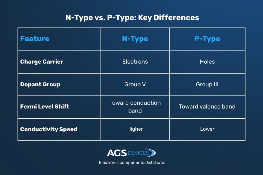
This comparison shows how their charge carriers and dopants impact performance
What are common examples of N-type semiconductors?
- Silicon doped with phosphorus: Microchips, MOSFETs
- Gallium nitride (GaN): Fast chargers, RF devices
- Indium phosphide (InP): Fiber optics, lasers
- Zinc oxide (ZnO): Transparent displays, UV sensors
Which best describes an example of an N-type semiconductor?
A good example is silicon doped with phosphorus. The phosphorus atom donates an extra electron, which increases the material’s conductivity and makes it suitable for use in logic circuits and microprocessors.
Where are N-type semiconductors used?
They’re found in nearly every modern electronic system:
- Medical electronics: Amplifiers in ECGs and imaging
- Automotive: Battery control systems, ECUs
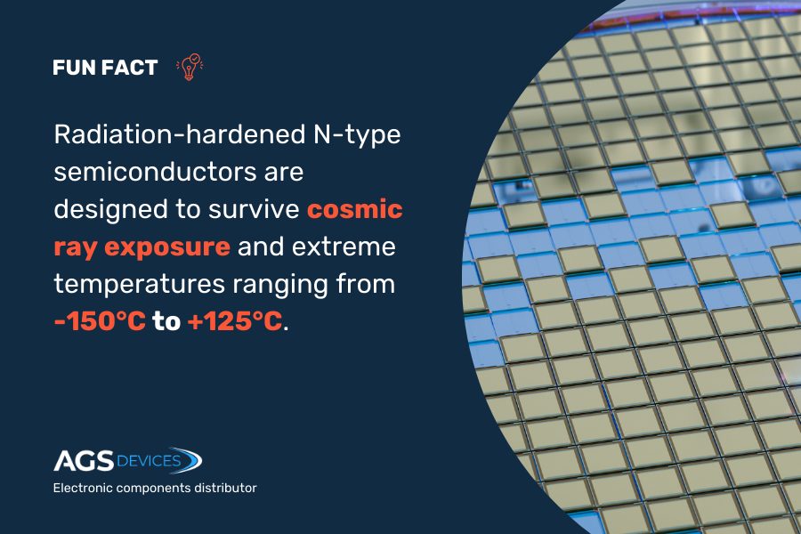
- Aerospace: Radiation-hardened processors