Semiconductor Doping: Key Takeaways
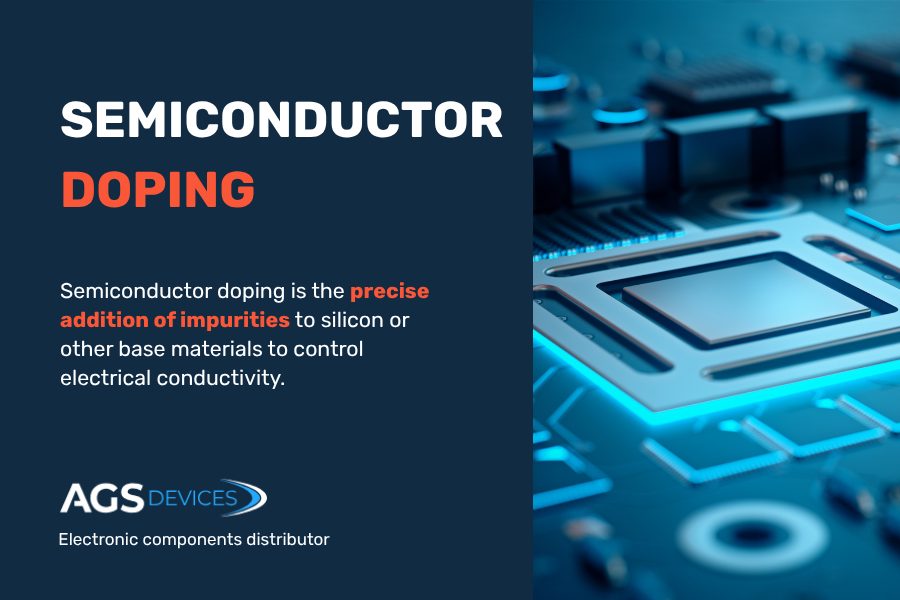
- Semiconductor doping is the process of intentionally adding impurity atoms (dopants) to pure silicon to control its conductivity and enable device functionality
- N-type and P-type doping introduces free electrons and holes, respectively, which are essential for creating diodes, transistors, and integrated circuits
- Common dopants include phosphorus, arsenic, and boron and each selected for specific electrical characteristics and compatibility with the substrate
- Doping methods such as ion implantation, thermal diffusion, and gas-phase deposition determine dopant depth, uniformity, and cost-effectiveness
- Doped semiconductors power critical devices like LEDs, CMOS chips, photodiodes, and RF modules that are used in automotive, aerospace, medical, and industrial applications
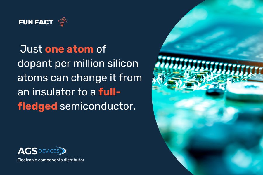
Over 90% of active electronic components rely on precisely doped semiconductors to function as intended.
That means the performance of everything from microcontrollers to photodiodes depends on how dopants are applied, and how well engineers understand the process.
In other words, behind every reliable chip is one quiet trick: adding just the right atoms.
In this guide, we’ll break down:
- What semiconductor doping is and why it matters
- The difference between n-type and p-type doping
- Common dopants and how they’re introduced into silicon
- Real-world applications across automotive, medical, aerospace, and industrial systems
Why Semiconductor Doping Is Essential
Semiconductor doping is essential because it transforms pure, non-conductive silicon into a versatile, controllable material that can conduct electricity as needed.
Without doping:
- Silicon behaves like an insulator with limited practical use in circuits
- Electronic devices couldn’t switch, amplify, or store data reliably
Doping introduces minute quantities of impurities, such as phosphorus (for electrons) or boron (for holes) to control charge carriers, enabling critical functions in:
- Transistors
- Photodetectors and solar cells
Why Doping Also Matters
Pure silicon forms a stable crystal structure but lacks mobile electrons or holes, limiting its usefulness in active devices.
Doping introduces free charge carriers:
- N-type doping adds electrons (using donor atoms like phosphorus or arsenic)
- P-type doping creates holes (using acceptor atoms like boron or gallium)
Key Terms To Know
- Intrinsic semiconductor: Pure, undoped material such as silicon or germanium
- Extrinsic semiconductor: A semiconductor that has been doped to improve conductivity
- Dopant: A foreign atom added to the crystal lattice to modify charge carrier behavior
- Charge carrier: A mobile electron or hole responsible for conducting current
Tip: A labeled diagram comparing intrinsic and doped silicon structures (n-type and p-type) enhances visual understanding.
Understanding N-Type and P-Type Doping
These two doping types create complementary electrical characteristics, enabling the formation of PN junctions, the core of nearly all semiconductor devices.
N-Type Doping: Adding Electrons
N-type semiconductors are created by introducing donor atoms, elements from Group V of the periodic table, into intrinsic silicon.
- Common dopants: Phosphorus (P), Arsenic (As), Antimony (Sb)
- Charge carriers: Free electrons (majority), holes (minority)
- Electrical behavior: Electrons move freely under an electric field, enhancing current flow
- Energy band view: Donor levels lie just below the conduction band, allowing easy promotion of electrons
- Application: Used in the source and drain of NMOS transistors, rectifiers, and cathodes in LEDs.
P-Type Doping: Creating Holes
P-type semiconductors are doped with acceptor atoms, which are elements from Group III, and they have only three valence electrons.
- Common dopants: Boron (B), Gallium (Ga), Indium (In)
- Charge carriers: Holes (majority), electrons (minority)
- Electrical behavior: Holes move through the lattice as nearby electrons jump to fill them
- Energy band view: Acceptor levels lie just above the valence band, easily accepting electrons
- Application: Found in anodes of diodes, base regions of BJTs, and PMOS transistor channels
Common Dopants and the Doping Process
Both material selection and process precision are critical to achieving consistent electrical performance in semiconductor devices.
Common Dopants Used in Semiconductors
Dopants are selected based on their valence electron count, compatibility with the semiconductor (usually silicon), and the desired electrical behavior.
Here are the most common dopant elements:
- Phosphorus (P): A Group V element with five valence electrons. Used for N-type doping, commonly in MOSFETs, CMOS logic, and high-speed diodes
- Arsenic (As): Also a Group V donor, offering low diffusion rates. Preferred in power semiconductors and low-diffusion junctions
- Antimony (Sb): Another N-type dopant with deeper junction profiles. Applied in RF devices and deep-level doping scenarios
- Boron (B): A Group III element with three valence electrons. Used for P-type doping, especially in BJT base regions and PMOS transistors
- Gallium (Ga): Another P-type dopant, commonly used in compound semiconductors. Suitable for optoelectronics and laser diodes
- Indium (In): A soft P-type dopant with applications in infrared sensing and precision analog components
Common Semiconductor Doping Methods
Each doping method offers trade-offs in precision, scalability, and cost.
Here are the four most common doping methods used in semiconductor manufacturing:
1. Ion Implantation
A high-precision technique widely used in modern IC fabrication.
It offers tight control over where and how dopants are placed, with key advantages including:
- Excellent control over dopant depth and concentration
- Minimal lateral diffusion, ideal for advanced nodes
- Requires post-implantation annealing to repair crystal damage
- Used extensively in CMOS, RF, and high-speed digital devices
2. Thermal Diffusion
A traditional method favored for deeper, uniform doping.
It relies on high heat to drive dopants into the wafer, resulting in:
- Broad doping profiles suitable for power applications
- Simpler equipment compared to ion implantation
- Effective for solar cells, analog ICs, and legacy devices
3. Spin-On or Liquid Doping
Best suited for prototyping and large-area applications.
The liquid dopant is applied and heat-treated, which allows for:
- Easy setup with low process complexity
- Shallow, uniform doping for low-spec layers
- Lower accuracy compared to implantation techniques
4. Gas-Phase Doping (CVD/PECVD)
Used during epitaxial growth in compound semiconductors.
Dopants are introduced during film deposition, enabling:
- Uniform, in-situ doping across complex structures
- High integration with materials like GaAs, SiC, and GaN
- Application in optoelectronics, RF, and LED devices
Applications of Doped Semiconductors
Doped semiconductors are the foundation of nearly every active electronic device.
Where Doped Semiconductors Are Used
From the LEDs in surgical tools to the RF chips in your car’s radar system, doped semiconductors are the invisible workhorses behind today’s smartest machines.
You can mostly find them in:
- Diodes: Formed by combining P-type and N-type materials to create a PN junction that allows the current to flow in one direction. They are used in rectifiers, LED lighting, and signal protection
- Transistors: Utilize layered doped regions (e.g., NPN or PNP in BJTs, source/drain in MOSFETs) to switch and amplify electrical signals. They are essential in everything from microprocessors to power modules
- Integrated circuits (ICs): Use millions (or billions) of doped transistors to perform logic operations, signal processing, and memory storage. They are found in processors, sensors, and embedded systems
- Photodetectors and photodiodes: Leverage doped junctions to convert light into electrical current, enabling cameras, optical sensors, and fiber-optic communication systems.
- Light Emitting Diodes (LEDs): Use heavily doped PN junctions to emit photons when forward biased. They are common in displays, automotive lighting, and medical devices
Industry Applications
Doped semiconductors are essential to device functionality in the following sectors:
- Automotive: Engine control units (ECUs), ADAS sensors, and electric powertrains depend on doped silicon for signal processing and power switching
- Aerospace and defense: Radiation-hardened ICs and RF modules use doped materials engineered for extreme environments
- Medical devices: Portable monitors, imaging systems, and medical electronic devices rely on doped semiconductors for accuracy, signal filtering, and power control
- Industrial automation: Motor drives, PLCs, and IoT sensors all depend on doped transistors and power devices for system stability and communication
Trusted Semiconductor Sourcing Starts With AGS Devices
At AGS Devices, we understand the critical role doped semiconductors play in powering high-performance components across automotive, aerospace, medical, and industrial sectors.
Whether you’re managing a new design, sourcing active components, or navigating obsolescence challenges, we deliver quality and continuity at every step.
We support your entire procurement workflow with:
Whether you’re building ICs, refining a BOM, or scaling production, AGS Devices is your sourcing partner for reliable, high-performance semiconductors.
Doping in Semiconductors FAQs
What is semiconductor doping?
Doping is the process of deliberately introducing impurity atoms called dopants into an intrinsic semiconductor (like silicon) to modify its electrical conductivity.
This turns the material into an N-type or P-type semiconductor, enabling controlled current flow in electronic devices.
What’s the difference between N-type and P-type doping?
N-type doping adds donor atoms (e.g., phosphorus) that contribute free electrons, making electrons the majority charge carriers.
P-type doping introduces acceptor atoms (e.g., boron) that create “holes” or positive charge carriers.
Together, they form the basis of PN junctions used in transistors and diodes.
What are the most common dopants used in silicon?
- N-type dopants: Phosphorus (P), Arsenic (As), Antimony (Sb)
- P-type dopants: Boron (B), Gallium (Ga), Indium (In)
These elements are chosen for their ability to integrate into the silicon lattice and modify its charge carrier balance without degrading structural integrity.
Why is doping necessary in semiconductors?
Without doping, pure semiconductors like silicon have very limited conductivity. Doping introduces free carriers (electrons or holes), allowing the material to conduct current in a predictable and controllable way, essential for building active electronic components.
What happens if a semiconductor isn’t doped?
An undoped (intrinsic) semiconductor has very few free charge carriers and cannot efficiently conduct electricity at room temperature. It behaves more like an insulator and is generally unsuitable for practical electronic applications unless modified by doping.
How is doping actually performed during manufacturing?
Common doping processes include:
- Ion implantation (high precision, used in ICs)
- Thermal diffusion (used in power devices)
- Spin-on doping (cost-effective for prototyping)
Each method controls the depth, concentration, and uniformity of dopant atoms in the wafer.